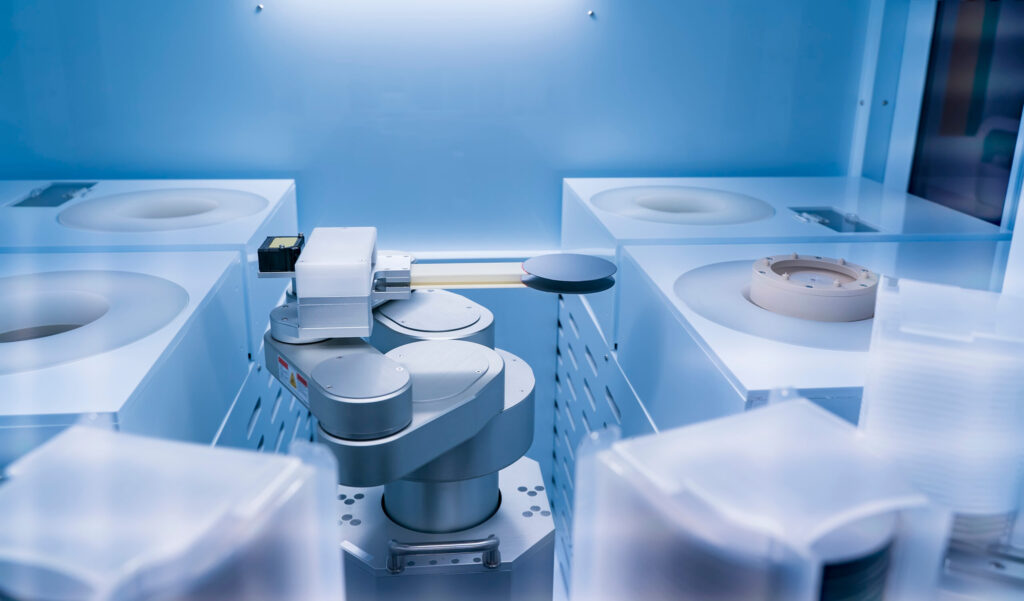
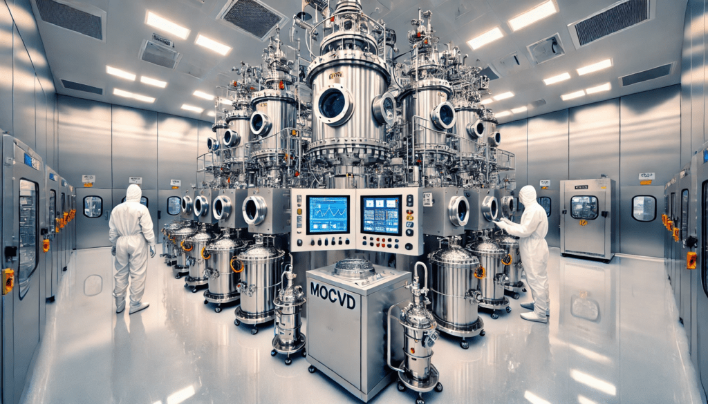
The semiconductor industry faces ongoing challenges in improving device performance, reducing manufacturing costs, and minimizing environmental impact. Traditional Metal-Organic Chemical Vapor Deposition (MOCVD) methods often struggle with precursor utilization, growth rates, and film uniformity, particularly for larger wafer sizes. At OTSON Technologies Corp, we are pioneering a novel hybrid MOCVD technique that integrates liquid precursor spray deposition with conventional gas-phase reactions and advanced AI-driven process controls. This innovative approach addresses the limitations of traditional MOCVD, offering a cost-effective and efficient solution for semiconductor device fabrication.
Key Benefits
Cost Reduction: Up to 80% reduction in cost per wafer due to enhanced precursor efficiency.
Higher Growth Rates: Achieving up to 200% faster growth rates compared to traditional MOCVD.
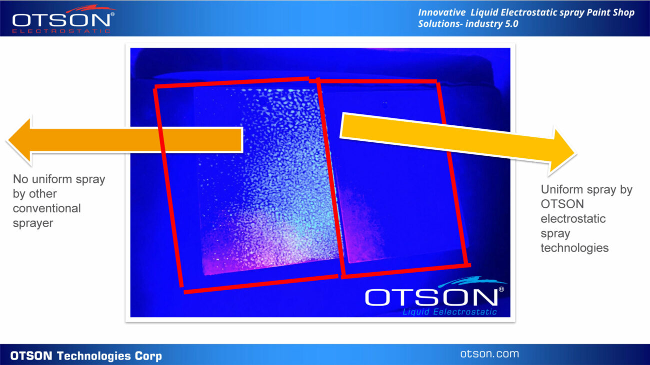
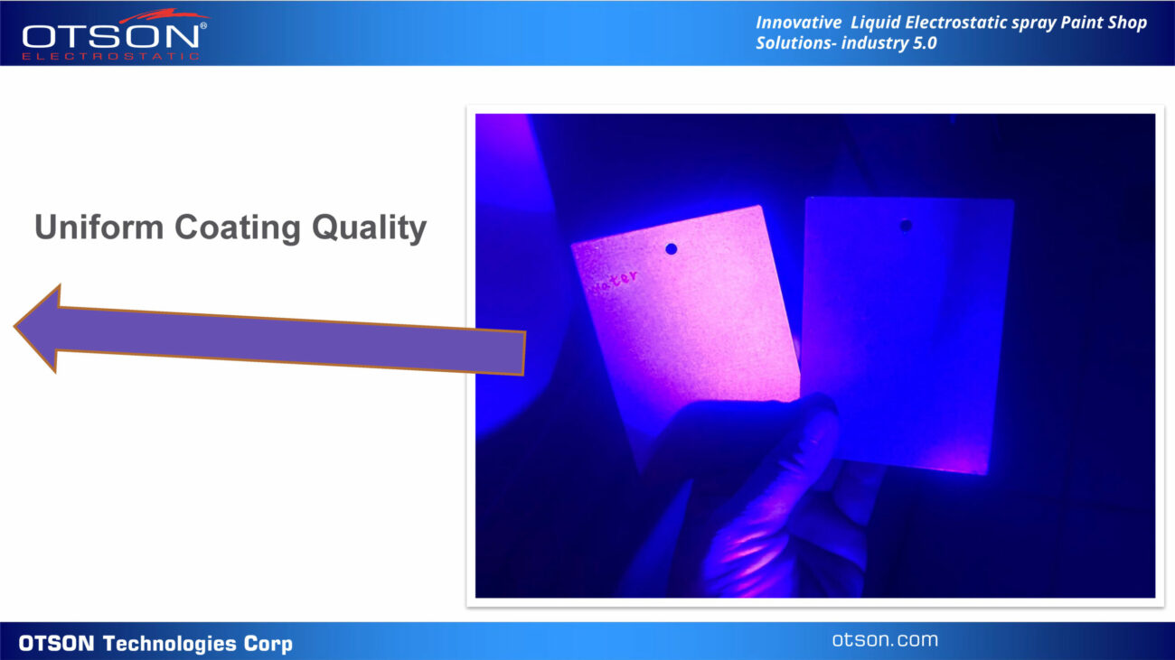
Improved Film Uniformity: Superior control over liquid precursor deposition, resulting in highly uniform films with reduced defect density.
AI-Driven Optimization: Utilizing artificial intelligence to monitor and optimize deposition processes in real-time, ensuring consistent quality and efficiency.
Here are the charts for the comparative analysis of the advantages of traditional MOCVD versus hybrid MOCVD:
Comparative Analysis: Precursor Utilization: This chart shows the precursor utilization percentages for both traditional and hybrid MOCVD methods across different materials and wafer sizes.
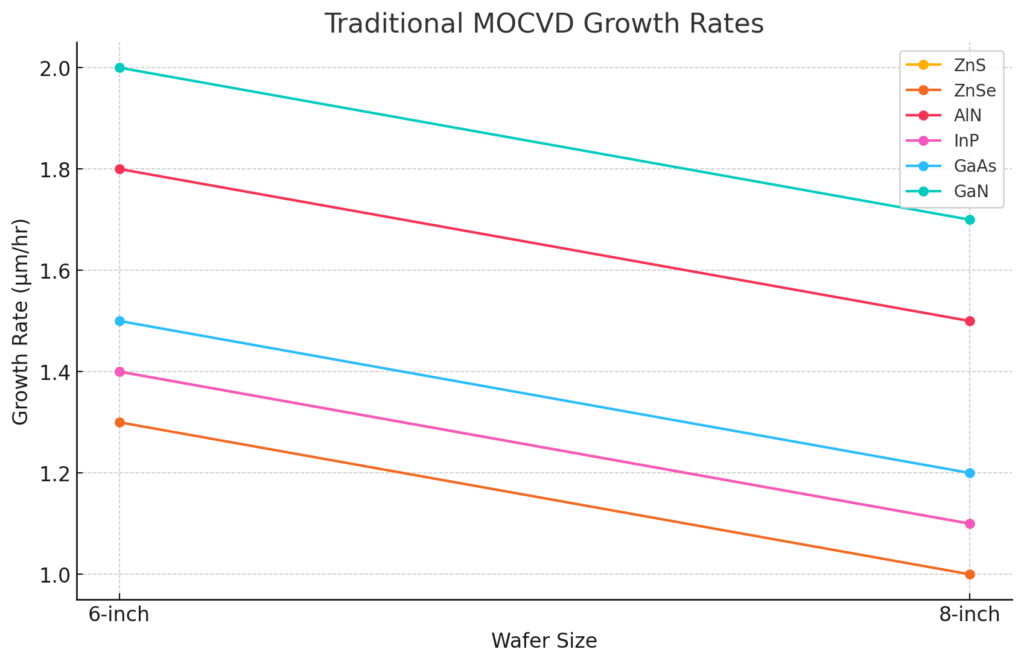
Comparative Analysis: Growth Rate: This chart illustrates the growth rates (µm/hour) for both traditional and hybrid MOCVD methods across various materials and wafer sizes.
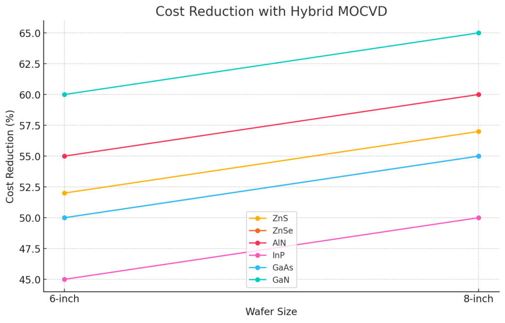
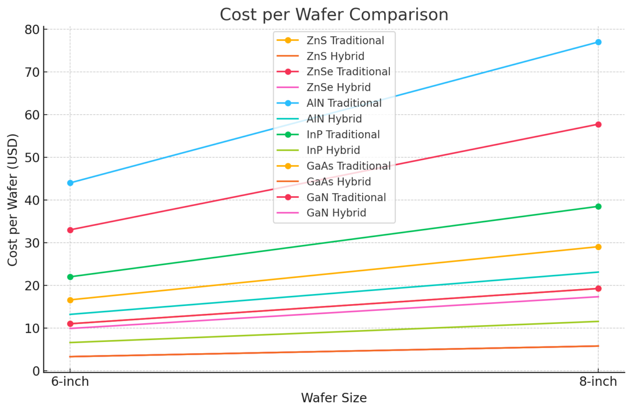
Comparative Analysis: Cost per Wafer: This chart highlights the cost per wafer (USD) for both traditional and hybrid MOCVD methods across different materials and wafer sizes.
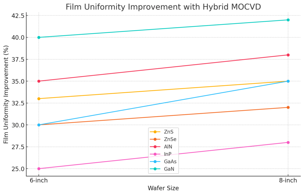
Improvement Comparison: This chart shows the improvement percentages for various metrics when using the hybrid MOCVD method compared to the traditional method across different materials and wafer sizes.
Impact on Industries
Our hybrid MOCVD technology promises to transform several key industries:
Consumer Electronics: Lower production costs for smartphones, laptops, TVs, and other devices make advanced technology more accessible to a wider population.
Electric Vehicles and Clean Energy: Enhanced production efficiency for semiconductors in EV batteries, solar panels, and power electronics supports a sustainable future by reducing costs and improving performance.
Data Centers: Faster production cycles and higher-quality semiconductors boost performance and energy efficiency in data centers, driving advancements in artificial intelligence and scientific research.
Healthcare: More affordable and sophisticated medical devices improve diagnostic tools, patient monitoring, and treatment effectiveness, leading to better healthcare outcomes.
Technical Overview
Our hybrid MOCVD technique is versatile and can be applied to a wide range of epitaxial types, including:
III-V Compounds:
Gallium Arsenide (GaAs)
Indium Phosphide (InP)
Gallium Nitride (GaN)
Aluminum Nitride (AlN)
II-VI Compounds:
Zinc Selenide (ZnSe)
Zinc Sulfide (ZnS)
Oxides:
Zinc Oxide (ZnO)
Gallium Oxide (Ga2O3)
2D Materials:
Graphene
Transition Metal Dichalcogenides (TMDs)
Perovskite Materials:
Lead Halide Perovskites
Mixed Halide Perovskites
These materials are crucial for various applications, including high-performance electronics, optoelectronics, power electronics, and advanced sensors.
Current Pain Points in MOCVD and MOVPE
MOCVD (Metal-Organic Chemical Vapor Deposition)
Precursor Utilization:
Issue: Traditional MOCVD systems often suffer from low precursor utilization efficiency. This leads to significant waste of costly precursor materials, increasing production costs.
Solution: OTSON’s hybrid MOCVD enhances precursor utilization by integrating liquid precursor spray deposition, ensuring more effective material usage.
Growth Rates:
Issue: Conventional MOCVD methods typically have slower growth rates, limiting production throughput and increasing manufacturing time.
Solution: Our hybrid approach achieves up to 200% faster growth rates, significantly boosting production capacity and efficiency.
Film Uniformity:
Issue: Achieving uniform thin films across large wafers is challenging with traditional MOCVD, leading to variations in device performance and yield.
Solution: The hybrid MOCVD technique provides superior control over deposition processes, resulting in highly uniform films with reduced defect density.
Energy Consumption:
Issue: High energy consumption due to the need for elevated temperatures in the gas-phase reactions, impacting operational costs and environmental footprint.
Solution: Our method reduces energy consumption by lowering the temperature required for initial film deposition, contributing to more sustainable manufacturing practices.
Process Control:
Issue: Traditional MOCVD relies heavily on operator expertise and manual adjustments, which can lead to inconsistencies.
Solution: Our AI-driven optimization continuously monitors and adjusts the process parameters in real-time, ensuring optimal conditions and consistent quality.
MOVPE (Metal-Organic Vapor Phase Epitaxy)
Precursor Delivery:
Issue: In MOVPE, the precursor delivery system can be complex and inefficient, leading to inconsistent material supply and film quality.
Solution: By integrating liquid precursor spray deposition, OTSON’s hybrid MOCVD ensures consistent and efficient precursor delivery.
Reactor Design:
Issue: MOVPE reactors often require complex designs to manage precursor flow and reaction kinetics, increasing system costs and maintenance needs.
Solution: Our hybrid system simplifies the reactor design while maintaining precise control over deposition processes.
Material Versatility:
Issue: MOVPE can be limited in terms of the range of materials it can effectively deposit, restricting its application scope.
Solution: The hybrid MOCVD technique is versatile, capable of depositing a wide range of materials, including III-V compounds, II-VI compounds, oxides, 2D materials, and perovskites.
Operational Costs:
Issue: The overall operational costs of MOVPE can be high due to precursor waste, energy consumption, and complex reactor maintenance.
Solution: OTSON’s hybrid MOCVD reduces operational costs through improved precursor utilization, energy efficiency, and simpler system maintenance.
Process Stability:
Issue: Maintaining stable process conditions over long production runs can be challenging in traditional MOVPE systems.
Solution: Our AI-driven system ensures continuous monitoring and adjustment, maintaining optimal conditions and enhancing process stability.
Transform semiconductor manufacturing with OTSON's hybrid MOCVD and AI-driven controls. Superior film uniformity, faster growth rates, and cost efficiency.
OTSON Electrostatic Spray Coating Technologies
In addition to our advanced MOCVD and MOVPE techniques, OTSON Technologies Corp offers state-of-the-art electrostatic spray coating technologies. These technologies are crucial for customizing and optimizing semiconductor equipment, ensuring high-quality finishes and efficient coating processes.
Key Electrostatic Spray Coating Products:
OTS-3000 Manual Liquid Electrostatic Spray Gun:
High transfer efficiency
Easy to clean
Ideal for precision coating applications
OTS-7800 Auto Electrostatic Spray Gun Robot Arm:
High efficiency
Large area coverage
Suitable for automated production lines
OTS-8000 Auto Electrostatic Spray Gun System:
High transfer efficiency
Flexible control
Perfect for complex coating tasks
OTS-5000 Auto Electrostatic Spray Disk System:
Even application
High transfer efficiency
Excellent for uniform coating
OTS-9000 Auto Electrostatic Spray Bell System:
High-quality finishes
Reduced overspray
Minimizes CO2 emissions
These electrostatic spray coating technologies are designed to meet the rigorous demands of semiconductor manufacturing, providing reliable and efficient solutions for coating and customization of MOCVD and MOVPE epitaxial equipment.
Market Potential
The hybrid MOCVD technology presents a significant market opportunity, particularly in high-demand sectors such as:
LEDs: Providing higher growth rates and improved film uniformity for large-area wafers, essential for high-brightness LEDs.
Power Electronics: Enhancing efficiency and performance of wide bandgap materials (e.g., GaN, SiC) for high-power and high-frequency applications.
Advanced Sensors: Enabling precise control over material properties for innovative sensor technologies.
Flexible Electronics: Supporting the growth of high-quality films on flexible substrates, paving the way for wearable devices and flexible displays.
Chip Applications
Our hybrid MOCVD technology can be used to fabricate various types of semiconductor chips, including:
Chip Type
Application Areas
Benefits
Epitaxial Types
Compounds
Microprocessors and Microcontrollers
Computers, smartphones, embedded systems
Improved film uniformity and faster production cycles
III-V Compounds, II-VI Compounds
GaAs, InP, ZnSe, ZnS
Power Management ICs
Power supply regulation in electronic devices, electric vehicles
Leveraging high-efficiency GaN and SiC materials
III-V Compounds
GaN, SiC
RF and Microwave Devices
Communication systems, radar
High-quality III-V compound semiconductors
III-V Compounds
GaAs, GaN
Optoelectronic Devices
LEDs, laser diodes, photodetectors
High-brightness and performance
III-V Compounds
GaAs, GaN
Sensors and MEMS
Automotive, industrial, consumer applications
Precise control over material properties
III-V Compounds, Oxides, 2D Materials
GaN, ZnO, Graphene, TMDs
Solar Cells
Photovoltaic devices
Enhancing efficiency and reducing costs
Perovskite Materials
Lead Halide Perovskites
Memory Chips
DRAM, SRAM, Flash memory
Impacting performance and reliability
III-V Compounds, II-VI Compounds
GaAs, InP, ZnSe, ZnS
Impact on Future Industrial and Consumer Applications
Industrial Applications
Increased Efficiency: The significant improvements in growth rates and cost efficiency will enable manufacturers to scale up production rapidly, meeting the growing demand for advanced semiconductor devices.
Enhanced Device Performance: Improved film uniformity and reduced defect density will lead to higher performance and reliability of semiconductor devices, crucial for industrial applications such as power electronics and RF devices.
Sustainability: Reduced energy consumption and precursor waste align with global sustainability goals, helping industries minimize their environmental impact.
Consumer Applications
Affordable Electronics: Lower production costs translate to more affordable consumer electronics, making advanced technology accessible to a broader audience.
Enhanced User Experience: Higher performance and reliability of semiconductor devices will result in better user experiences in smartphones, laptops, and other consumer gadgets.
Innovation in Wearables: The ability to produce high-quality films on flexible substrates will drive innovation in wearable technology, leading to new and exciting consumer products.
Impact on AI Industry
Data Center Efficiency: Faster production cycles and higher-quality semiconductors will boost the performance and energy efficiency of data centers, which are the backbone of AI infrastructure.
Advanced AI Chips: Improved semiconductor manufacturing processes will enable the production of advanced AI chips with higher processing power and efficiency, driving advancements in AI research and applications.
Scalability: Enhanced manufacturing efficiency and reduced costs will make it feasible to scale up the production of AI chips, meeting the increasing demand for AI-powered devices and applications.
Proven Results
Our hybrid MOCVD technology has significantly improved growth rates, cost efficiency, and film quality. Real-world applications and rigorous testing validate these benefits, making it a reliable choice for your semiconductor manufacturing needs.
AI-Driven Optimization
Our AI-driven optimization continuously monitors and adjusts process parameters in real time, ensuring optimal conditions and consistent quality. This advanced capability enhances process stability and efficiency, giving you a competitive edge in semiconductor manufacturing. Tailored Solutions
We understand that every business has unique requirements. Our team works closely with you to customize our hybrid MOCVD systems to meet your specific production goals and material needs.
Comprehensive Support
OTSON Technologies Corp is committed to ensuring your success from initial consultation to ongoing support. We offer comprehensive training, technical support, and maintenance services to help you maximize the benefits of our technology.
Sustainable Manufacturing
Our hybrid MOCVD process enhances efficiency and aligns with sustainable manufacturing practices by reducing precursor waste and energy consumption. This helps you achieve your environmental goals while staying competitive.
Contact Us
Are you ready to revolutionize your semiconductor manufacturing process? Partner with OTSON Technologies Corp and leverage our advanced hybrid MOCVD technology for unparalleled performance and cost savings.
Contact us today to learn more about our solutions and how we can help you achieve your production goals.
We use cookies to ensure that we give you the best experience on our website. If you continue to use this site we will assume that you are happy with it.